In Clock Domain Crossing (CDC) Techniques – Part 1, I briefly discussed metastability and two methods to safely synchronize a single bit. While those techniques are commonly used, in many applications we need to synchronize multiple control or data bits, like an encoded state or a data bus. Synchronizing multiple bits brings a host of other potential problems that need to be carefully examined, and solutions that build upon the basic blocks we discussed in part 1.
The concepts in this article are again mostly taken from Cliff Cumming's very comprehensive paper Clock Domain Crossing (CDC) Design & Verification Techniques Using SystemVerilog. I highly recommend taking an hour or two to read through it.
Problems With Passing Multiple Control Signals Across Clock Domain Crossing (CDC)
The fundamental problem with passing multiple bits is if they are synchronized individually, they cannot be guaranteed to arrive in the destination clock domain on the same clock edge. When the individual bits are launched from the source clock domain, they may be skewed relative to each other due to trace length, process variation, etc. Since in an asynchronous clock domain crossing (CDC) the destination clock can have every possible alignment relative to the source clock (and relative to the skewed data bits), the destination clock can (and will) sample at a time when not all the bits are at their stable final values. Therefore synchronizing individual bits of a multi-bit signal is not sufficient! Let’s look at several potential problems.
Two simultaneously required signals
The waveform below shows how data skew from the source clock domain can cause two signals to arrive in different clock cycles in the destination domain, if they are synchronized individually using two flip-flop synchronizers. Don’t do this!

Two sequenced signals
Individually synchronizing two signals that require precise sequencing across an asynchronous clock domain crossing (CDC) is a recipe for disaster. In fact a recent ASIC project at work had a problem like this that resulted in a chip that only booted 50% of the time, months of debug, and finally a respin (we make mistakes too).
The waveform below shows how two separate signals that are intended to arrive 1 cycle apart in the destination domain, can actually arrive either 1 or 2 cycles apart depending on data skew. It’s difficult to even analyze the frequency difference from the source to destination clock domain and come up with a potential sequence that may work… Just don’t do this. There are better ways!

Encoded control signals
There are many scenarios where you may want to pass a multi-bit signal across a clock domain crossing (CDC), such as an encoded signal. By now we understand the potential problem, right? Due to data skew, the different bits may take different number of cycles to synchronize, and we may not be able to read the same encoded value on the destination clock domain. You may get away with using a simple two flip-flop synchronizer if you know there will be sufficient time for the signal to settle before reading the synchronized value (like a relatively static encoded status signal). But it’s still not the best practice.
Solutions For Passing Multiple Signals Across Clock Domain Crossing (CDC)
So how do we deal with synchronizing multiple signals? There are at least several solutions with different levels of complexity:
- Multi-bit signal consolidation
- Multi-cycle path (MCP) formulation without feedback
- Multi-cycle path (MCP) formulation with feedback acknowledge
- Dual-Clock Asynchronous FIFO
- Two-Deep FIFO
Multi-cycle path (MCP) formulation is a particularly interesting and widely applicable solution. It refers to sending unsynchronized data from the source clock domain to the destination clock domain, paired with a synchronized control (e.g. a load enable) signal. The data and control signals are sent simultaneously from the source clock domain. The data signals do not go through any synchronization, but go straight into a multi-bit flip-flop in the destination clock domain. The control signal is synchronized through a two-flip-flop synchronizer, then used to load the unsynchronized data into the flip-flops in the destination clock domain. This allows the data signals to settle (while the control signal is being synchronized), and captured together on a single clock edge. We will get into two variations of this technique in later sections.
Multi-bit signal consolidation
Consolidating multiple bits across clock domain crossing (CDC) into one is more of a best practice, than a technique. It’s always good to reduce as much as possible the number of signals that need to cross a clock domain crossing (CDC). However, this can be applied directly to the problem of sequencing two signals into the destination clock domain. A single signal can be synchronized across the clock domain crossing (CDC), and the two sequenced signals can be recreated in the destination clock domain once the synchronizing signal is received.
Multi-cycle path (MCP) formulation without feedback
The multi-cycle path (MCP) synchronizer is comprised of several components:
- Logic that converts a synchronization event from source clock domain to a toggle to pass across the clock domain crossing (CDC)
- Logic that converts the toggle into a load pulse in the destination domain
- Flip-flops to capture the unsynchronized data bits
One key idea in this design is that the synchronization event (a pulse) is converted into a single toggle (either low to high, or high to low) before being synchronized into the destination clock domain. Each toggle represents one event. You need to be careful when resetting the synchronizer such that no unintended events are generated (i.e. if the source domain is reset on its own, and the toggle signal goes from high to low due to reset).
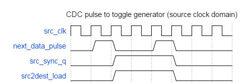
Source clock domain event to toggle generator

The following circuit resides in the source clock domain, and converts an event that needs to traverse the clock domain crossing (CDC) into a toggle, which cannot be missed due to sampling in the destination clock domain.
Destination clock domain toggle to load pulse generator

Next, we need a circuit in the destination clock domain to convert the toggle back into a pulse to capture the multi-bit signal.

Finally, putting the entire synchronizer circuit together, we get the following.

Notice the multi-bit data signal passes straight from source (clock) flip-flop to destination (clock) flip-flop to avoid problems with synchronizing multiple bits. A single control signal is synchronized to allow time for the multi-bit data to settle from possible metastable state. The load pulse from the source clock domain first gets converted into a toggle. The toggle is synchronized across the clock domain crossing (CDC), then gets converted back to a load pulse in the destination clock domain. Finally that load pulse is used to load the multi-bit data signal into flip-flops in the destination clock domain.
Rate of Synchronization
Initially you may think that the the toggle synchronizer eliminates the problem of a missing pulse when crossing from a fast clock to a slow clock domain. However, there is a limitation of the rate of how often data can be synchronized across the synchronizer. If you look at the complete circuit, the input data has to be held until the the synchronization pulse loads the data in the destination clock domain. The whole process takes at least two destination clocks. Therefore to use this circuit, you must be certain that the input data only needs to be synchronized not more than once every three destination clock cycles. If you are unsure, then a more advanced synchronization circuit like the synchronizer with feedback acknowledgement or Dual-Clock Asynchronous FIFO should be used.
Conclusion
Passing multiple signals across an asynchronous clock domain crossing (CDC) can become a recipe for disaster if not done properly. This article described some potential pitfalls, and one very effective technique called multi-cycle path (MCP) formulation to synchronize multiple bits across a clock domain crossing (CDC). There is one missing piece, however. How does logic in the source clock domain know when it is safe to send another piece of data? In Part 3 of the series, I will put in the final piece and enhance the multi-cycle path (MCP) synchronizer with feedback acknowledgement.
References
- Metastability and Synchronizers: A Tutorial
- Synthesis and Scripting Techniques for Designing Multi-Asynchronous Clock Designs
- Clock Domain Crossing (CDC) Design & Verification Techniques Using SystemVerilog
- Pragmatic Simulation-Based Verification of Clock Domain Crossing Signals and Jitter Using SystemVerilog Assertions
- Crossing the abyss: asynchronous signals in a synchronous world
Sample Source Code
The accompanying source code for this article is the multi-bit MCP synchronizer without feedback design and testbench, which generates the following waveform when run. Download and run the code to see how it works!

Hi Jason
First of all, I want to thank you for your 3 parts-series , which is very helpful for me.
But I noticed a discrepancy in the SystemVerilog code, in the sync_mcp_src, you made the “src2dest_ldtoggle <= src2dest_ldtoggle ^ src_data_valid“ excute under the dest_clk, shouldn't it be combinational?
And the waveforms of the above code shows a clk delay comparing to the waveforms in your post
Sorry about the previous post, there are some typos. The module should be sync_mcp_dest
But I noticed a discrepancy in the SystemVerilog code, in the sync_mcp_sedt, you made the “data_valid_sync <= ldtoggle_sync ^ ldtoggle_sync_d1“ excute under the dest_clk, shouldn't it be combinational?
Hi Pan. Yes you’re right! My code didn’t match the diagram I drew, and was inserting an unnecessary extra cycle before the data appeared on the destination side. I’ve fixed the code and waveform. Thanks for pointing that out!
The toggle synchronizer without feedback does not really work for negative pulses, right ?
Besides, http://www.verilogpro.com/clock-domain-crossing-part-3/ returns 404 status
Hi Promach. If you’re talking about the Multi-cycle path (MCP) formulation without feedback, it should work for sending both ones and zeros. There are two different paths through the synchronizer—1) the data path where the data to be synchronized is sent to the destination and can be either one or zero, 2) the synchronization event indication. In this design, the source logic must create a single cycle positive pulse to indicate there is data on the data path to synchronize.
Thanks for your useful reply.
As in https://i.stack.imgur.com/lXrCw.jpg extracted from https://inst.eecs.berkeley.edu/~cs150/sp10/Collections/Papers/ClockCrossing.pdf#page=3 , it seems to me that toggle synchronizer needs to impose that input pulses must have a minimum spacing between pulses equal to two synchronizer clock periods.
The article also mentioned “This problem is more severe when the clock period of input pulse is greater than twice the synchronizer clock period ”
Do you have any comments about this ?
Thanks for the link to the paper. It’s always good to get another perspective on how to design these circuits. I’ll add it to the reference section as well.
When synchronizing a signal, the first considerations must always be the relative frequencies of the two domains, and how frequently data needs to be transferred between them (the rate of synchronization). I think the paper you referenced mentions a two destination cycle limitation to ensure the output pulse is distinct and single cycle. Yes there is the same limitation in my MCP without feedback circuit because the output pulse is used to load the output flip-flop, and the source flip-flops cannot change until this occurs. So to use the MCP without feedback circuit you must be sure that the input data rate is fairly slow. If you are unsure or if the design requires more frequent synchronization, then the feedback synchronizer or asynchronous FIFO should be used.
As for the sentence from the article, I wonder if he meant the frequency of input clock is greater than twice the synchronizer clock. I don’t see why a long input pulse would be a problem for this toggle synchronizer.