In Clock Domain Crossing (CDC) Design – Part 2, I discussed potential problems with passing multiple signals across a clock domain, and one effective and safe way to do so. That circuit, however, does hot handle the case when the destination side logic cannot accept data and needs to back-pressure the source side. The two feedback schemes in this article add this final piece.
The concepts in this article are again taken from Cliff Cummings’ very comprehensive paper Clock Domain Crossing (CDC) Design & Verification Techniques Using SystemVerilog. I highly recommend taking an hour or two to read through it.
Multi-cycle path (MCP) formulation with feedback
How can the source domain logic know when it is safe to send the next piece of data to the synchronizer? It can wait a fixed number of cycles, which can be determined from the synchronizer circuit. But a better way is to have logic in the synchronizer to indicate this to the source domain. The following figure illustrates how this can be done. Compared to the MCP without feedback circuit, it adds a 1-bit finite state machine (FSM) to indicate to the source domain whether the synchronizer is ready to accept a new piece of data.
The 1-bit FSM has 2 states, 2 inputs, and 1 output (besides clock and reset).
- States: Idle, Busy
- Inputs: src_send, src_ack
- Output: src_rdy
The logic is simple. src_send causes the FSM to transition to Busy, src_ack causes the FSM to transition back to Idle. src_rdy output is 1 when Idle, and 0 when Busy. The user logic outside the synchronizer needs to monitor these signals to determine when it is safe to send a new piece of data.
Multi-cycle path (MCP) formulation with feedback acknowledge
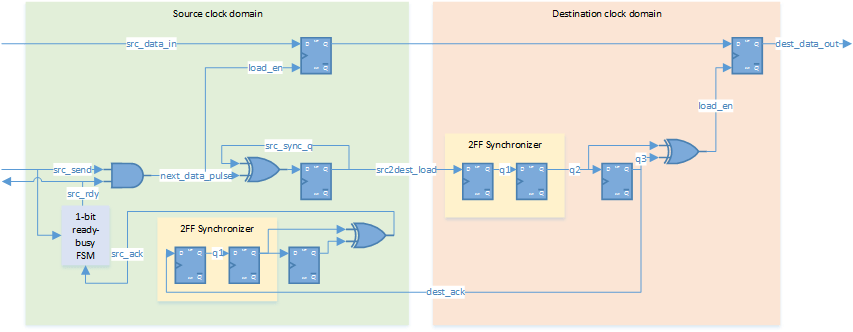
What if the destination domain further needs to back-pressure data from the source domain? To do so, the destination domain will need control over when to send feedback acknowledgement to the source domain. This can be accomplished by adding a similar 1-bit FSM in the destination side of the synchronizer. This addition allows the destination clock domain to throttle the source domain to not send any data until the destination domain logic is ready. The following figure illustrates this design.

And there you have it. A complete multi-bit synchronizer solution with handshaking. Note that this particular design is slightly different from the design described in Cliff Cummings’ paper. I have changed the destination side to output data on dest_data_out as soon as available, rather than waiting for an external signal to load the data like the bload signal in Cliff Cummings’ circuit. It doesn’t seem efficient to me to incur another cycle to make the data available.
I apologize that the diagram is a bit messy (if anyone knows of a better circuit drawing tool, please let me know). The source code will be provided below so you can study that in detail.
1-Deep Asynchronous FIFO
Obviously the dual-clock asynchronous FIFO can also be used to pass multiple bits across a clock domain crossing (CDC). What is interesting, however, is a 1-deep asynchronous FIFO (which actually has space for 2 entries, but will only ever fill 1 at a time) provides the same feedback acknowledge capability as the MCP formulation circuit above, but with 1 cycle lower latency on both the send and feedback paths.
In this configuration, pointers to the FIFO become single bit only, and toggle between 0 and 1. Read and write pointer comparison is redefined to produce a single bit value that indicates either ready to receive data (FIFO is empty, pointers equal) or not ready to receive data (FIFO is not empty, pointers not equal). Notice that when the logic indicates not ready, the write pointer has already incremented and is pointing to the next entry of the 2-entry storage to store data. Also, the FIFO read/write pointer circuitry essentially replaces the 1-bit state machine in the MCP formulation feedback scheme, therefore requiring 1 less step and 1 less cycle.
Conclusion
Over this 3-part series, we have looked at potential problems and proven design techniques to handle clock domain crossing (CDC) logic for single-bit signals (Part 1), and multi-bit signals (Part 2, and Part 3). Cliff Cummings gives a good summary from his paper:
Recommended 1-bit CDC techniques
- Register the signal in the source domain to remove combinational settling (glitches)
- Synchronize the signal into the destination domain
Recommended multi-bit CDC techniques
- Consolidate multiple signals into a 1-bit representation, then synchronize the 1-bit signal
- Use multi-cycle path (MCP) formulation to pass multi-bit data buses
- Use asynchronous FIFOs to pass multi-bit data or control buses
- Use gray code counters
Writing about this topic has been a much bigger (but also more rewarding) undertaking than I imagined. I must confess I’m still relatively new to asynchronous designs. So if you have any experience or design techniques to share, please leave a comment below! How about investigating clock domain crossing verification next?
References
- Clock Domain Crossing (CDC) Design & Verification Techniques Using SystemVerilog
- Simulation and Synthesis Techniques for Asynchronous FIFO Design
Sample Source Code
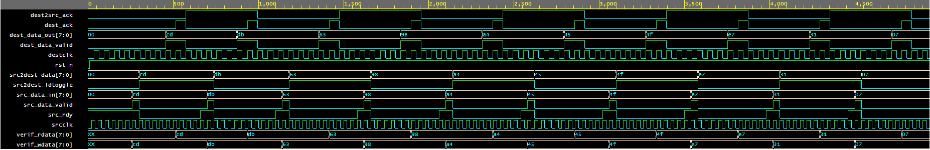
The accompanying source code for this article is the MCP feedback acknowledge synchronizer design and testbench, which generates the following waveform when run. Download and run the code to see how it works!
Hi, can you please re-verify your code uploaded here as it is giving Error: Checking failed.
Hi. What simulator are you running the code with? I checked the code with VCS on http://www.edaplayground.com . Can you try running it there?
Your modification from Cliff Cumming’s paper, to output data on dest_data_out as soon as available won’t be a good idea every time. What if before asserting dest_ack signal, destination domain is still using the previously captured data directly from dest_data_out signal? In that case, you might need extra register (with enable logic) to hold the older data when you capture the new asynchronous data as soon as it’s available (but before the assertion of dest_ack signal).
Thanks for your thoughtful comment. Looking at the paper again it seems I did modify the circuit slightly on the receiver side. You’re absolutely right. I’m more used to a feed forward kind of design, so my design goal was to present data on the destination domain together with asserting dest_valid. With that, my assumption was the destination logic would not assert dest_ack until it has captured dest_data_out signal. But I see how the original circuit could have potentially saved an extra capture flop to capture dest_data_out.
Awesome work. One of the best out there in CDC. Please keep up the good work!
Thanks a lot.
Sudeendra.